Common Emitter Amplifier Circuit Diagram — Free & Editable
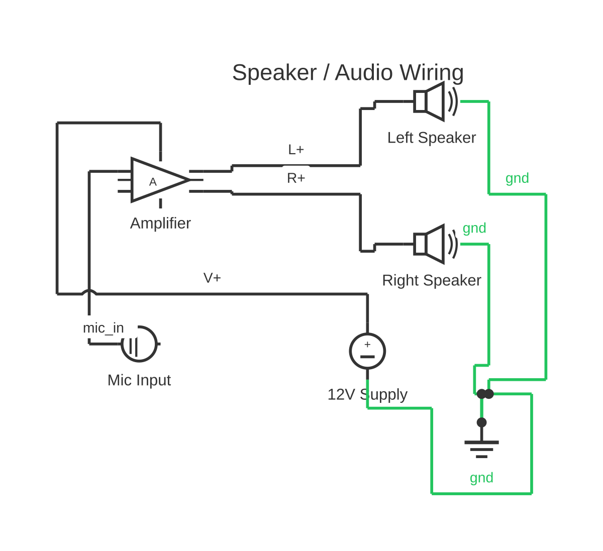
This is a free printable common emitter amplifier circuit diagram: download the diagram as SVG or open it and print to paper or PDF.
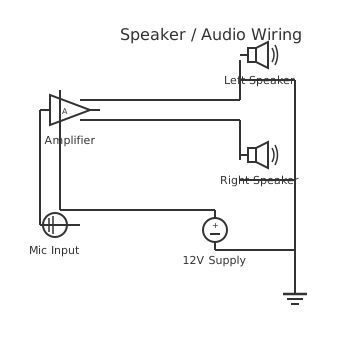
The current drawing contains 6 components and 7 routed connections, including 1 × Amplifier (Amplifier Block), 1 × Left Speaker (Speaker), 1 × Right Speaker (Speaker), 1 × Mic Input (Microphone) and 1 × 12V Supply (DC voltage source). Use it to inspect the shown topology, then confirm ratings and terminal assignments against the equipment documentation for your installation.
Diagram checks and scope
- Components
- 6
- Wired connections
- 7
- Automated check
- Automated pin, route, source, and topology checks passed; this is not a safety certification.
What this Common Emitter Amplifier Circuit Diagram drawing contains. The rendered example uses 1 × Amplifier (Amplifier Block), 1 × Left Speaker (Speaker), 1 × Right Speaker (Speaker), 1 × Mic Input (Microphone), 1 × 12V Supply (DC voltage source) and 1 × circuit reference. Audio paths depend on channel identity, polarity, shielding and the load impedance presented to each amplifier output. The component names in the list below come from the editable canvas, while the wire summary comes from the saved start and end terminals. This makes the written explanation auditable against the image instead of presenting an unrelated stock circuit.
Reading the stored graph from terminal to terminal gives this sequence: 1. Amplifier out1 terminal connects to Left Speaker pos terminal on the L+ net. 2. Amplifier out2 terminal connects to Right Speaker pos terminal on the R+ net. 3. Mic Input pos terminal connects to Amplifier in1 terminal on the mic_in net. 4. 12V Supply pos terminal connects to Amplifier vcc terminal on the V+ net. 5. Left Speaker neg terminal connects to circuit reference gnd terminal on the gnd net. 6. Right Speaker neg terminal connects to circuit reference gnd terminal on the gnd net. 7. 12V Supply neg terminal connects to circuit reference gnd terminal on the gnd net. Its named nets are “L+”, “R+”, “mic_in”, “V+” and “gnd”. A line joining two terminals records electrical continuity in this reference; visual proximity alone does not create a connection. Junctions, bridges and terminal labels therefore matter when the drawing is edited or exported.
Follow each signal conductor from source to destination while keeping channel returns and shields explicit. Series and parallel speaker arrangements change total impedance; bridged outputs must not be treated as grounded single-ended outputs. In this particular graph, the first visible path is Amplifier out1 terminal connects to Left Speaker pos terminal on the L+ net., Amplifier out2 terminal connects to Right Speaker pos terminal on the R+ net., Mic Input pos terminal connects to Amplifier in1 terminal on the mic_in net. and 12V Supply pos terminal connects to Amplifier vcc terminal on the V+ net.. Follow the remaining rows in the connection table before changing a symbol or moving a conductor, because a neat layout is not evidence that a terminal function is correct.
Confirm connector orientation, channel assignment, amplifier topology, permitted load impedance, shield termination and cable type. Measure passive continuity only with equipment powered down. Automated validation checks that component IDs and terminal IDs exist, routes terminate on pins, the graph has a recognized source, and the saved topology has no blocking structural fault. It does not determine conductor size, protective-device rating, fault current, insulation class, environmental suitability or compliance with local rules. Those decisions require project values and the current primary documentation.
How to wire common emitter amplifier circuit diagram
- Read the Common Emitter Amplifier Circuit Diagram source path For this common emitter amplifier circuit diagram, begin at Amplifier (Amplifier Block) and trace every stored terminal pair toward the load or output; do not infer continuity from lines that merely cross.
- Match every terminal name Compare the Common Emitter Amplifier Circuit Diagram terminal labels shown in the connection table with the current device or standard documentation before assigning real conductors.
- Set project-specific ratings Replace placeholder values in the common emitter amplifier circuit diagram with verified voltage, current, protection, conductor and environmental data for the actual installation.
- Run the electrical checks again After editing Left Speaker (Speaker) or any route, validate the graph and inspect every reported open terminal, source fault, collision and disconnected island.
- Release a controlled copy Export the revised Common Emitter Amplifier Circuit Diagram drawing only after a competent reviewer has compared it with the bill of materials, manufacturer documents and applicable rules.
Specifications
| Topic | Common Emitter Amplifier Circuit Diagram |
|---|---|
| Components shown | 6 |
| Routed connections | 7 |
| Named nets | L+, R+, mic_in, V+, gnd |
| Verification scope | Stored pins, routes, source path and graph topology |
Safety warnings
- Power down amplifiers before changing speaker or signal wiring.
- Keep high-level speaker wiring separated from low-level inputs to reduce damage and noise risk.
Tools needed
- The current manufacturer datasheet, connector schedule or applicable standard for every real device
- A suitable meter and proving method for the voltage class being worked on
- The editor validation report and a controlled terminal or wire schedule
Common mistakes
- Treating the common emitter amplifier circuit diagram illustration as proof of a manufacturer pinout or conductor rating when those values are not encoded in the graph.
- Connecting by component position or wire colour instead of checking the named terminals in the Common Emitter Amplifier Circuit Diagram connection path.
- Joining amplifier negative outputs or cable shields as a universal ground without checking whether the output is bridged or balanced.
Troubleshooting
- The Common Emitter Amplifier Circuit Diagram path appears open
- Cause: A route ends on the wrong pin, a terminal was renamed, or a required return path is absent. Fix: Trace the connection rows in order, restore the documented terminal mapping, and run validation again.
- The edited drawing passes visually but validation fails
- Cause: A conductor may stop off-pin, cross a component body, create a source short or leave a disconnected island. Fix: Open each blocking finding, correct the referenced component or route, then re-run the topology check before export.
- The real equipment behaves differently
- Cause: The stored reference does not match the exact model, revision, supply or contact state. Fix: De-energize safely, return to the current primary documentation, and revise the symbol terminals and values before further testing.
Frequently asked questions
What exactly is verified on this common emitter amplifier circuit diagram?
The saved Common Emitter Amplifier Circuit Diagram graph is checked for known components and terminals, pin-snapped routes, a recognizable source path and blocking topology defects. Exact equipment ratings and manufacturer assignments are outside that automated scope.
Which components are actually shown in this Common Emitter Amplifier Circuit Diagram diagram?
The current editable graph contains 1 × Amplifier (Amplifier Block), 1 × Left Speaker (Speaker), 1 × Right Speaker (Speaker), 1 × Mic Input (Microphone), 1 × 12V Supply (DC voltage source) and 1 × circuit reference. The bill of materials on this page is derived from those saved symbols rather than a generic shopping list.
How are the common emitter amplifier circuit diagram connections documented?
The graph contains 7 terminal-to-terminal links. The first path shown is Amplifier out1 terminal connects to Left Speaker pos terminal on the L+ net.
Can I use the drawing as an installation instruction?
Use it as an editable reference and review aid. Verify the exact equipment documentation, ratings, protection, conductor selection and local requirements before construction or release.
Sources and verification
Review status: Not independently reviewed. Automated topology checks confirm stored terminals and routes, not the correctness of manufacturer pin assignments, ratings, regional codes, or installation decisions. Verify those claims against the current primary documentation before use.
- IEC 61082-1:2014 — Rules for electrotechnical documents — International Electrotechnical Commission. Supports: General diagram, drawing, table, and reference-designation presentation conventions. Checked 2026-07-15.
Related diagrams
- 200w amplifier circuit diagram
- audio amplifier circuit diagram
- inverting amplifier circuit diagram
- non inverting amplifier circuit diagram
- power amplifier circuit diagram
- simple amplifier circuit diagram