How to Read a Schematic Diagram: Every Symbol, Rule, and Workflow
This is a free printable how to read a schematic: download the diagram as SVG or open it and print to paper or PDF.
A schematic diagram is the universal language of electronics — it shows how a circuit works using standardised symbols and connections, completely independent of how the components are physically arranged on a PCB or in an enclosure. Learning to read schematics unlocks the ability to build circuits from designs, troubleshoot malfunctions at the component level, and interpret any manufacturer datasheet or application note. This guide covers every symbol category, the ANSI vs IEC difference, net label topology, reference designators, and a proven 7-step reading workflow.
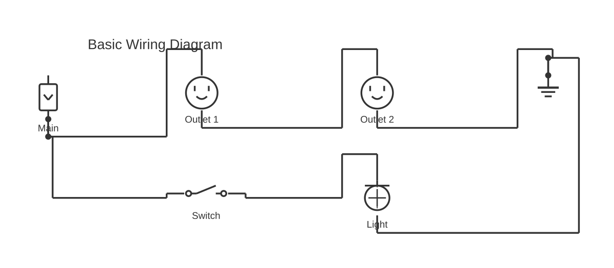
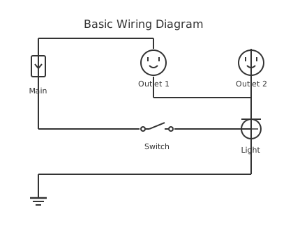
A schematic is not a wiring diagram, and it is not a PCB layout. Understanding the differences between all three is the essential first step for any reader. A schematic (circuit diagram) shows every electrical component and connection using standardised graphic symbols, with no regard for physical placement or real-world routing. It answers the question: how does this circuit work? A wiring diagram retains the schematic's symbolic language but also encodes physical routing, terminal numbers, and panel layout — it answers the question: how is this circuit installed? A PCB layout shows the actual copper traces, pad geometry, and component footprints on a circuit board — it answers the question: where are the components placed and how are they connected physically? An electronics engineer works primarily with schematics and PCB layouts; an installation technician works primarily with wiring diagrams. Many practitioners need to move fluently between all three.
Schematics are organised to be read from left to right and top to bottom, following the flow of signals and power. The power supply rail (VCC, VDD, or +5V) typically runs along the top of the schematic, and the ground reference (GND, 0V) runs along the bottom. Signal flow moves left to right: inputs enter from the left edge, pass through processing stages, and outputs exit from the right edge. This convention is universal across electronic schematics regardless of whether they are drawn to ANSI/IEEE 315, IEC 60617, or no specific standard. Complex schematics are divided into functional blocks — power supply, microcontroller, RF section, analogue front end — and reading them block by block rather than component by component is the key to understanding large designs.
The biggest source of confusion when learning to read schematics is the existence of two parallel symbol systems. IEEE 315 / ANSI Y32.2 is the North American standard: it uses a zigzag line for resistors, specific triangle shapes for logic gates, and certain transistor conventions. IEC 60617 is the international standard: it uses a rectangle for resistors, different gate body shapes, and a slightly different set of component outlines. Most commercial PCB design software (KiCad, Eagle/Autodesk, Altium Designer) allows schematic libraries in either standard, and many real-world schematics mix both because engineers from different countries have contributed to the same design. The most commonly encountered ANSI/IEC difference is the resistor: if you see a zigzag, you are in ANSI territory; if you see a plain rectangle, you are in IEC territory. A capacitor's polarized variant uses a curved plate (ANSI) or may use a filled plate (some IEC variants). Always check the schematic's notes for a declared standard before assuming.
Passive components form the foundation of every schematic. Resistors limit current and set biasing conditions; their value is labelled in ohms (Ω, kΩ, MΩ) beside the symbol. Capacitors store charge and filter signals; values appear in farads (pF, nF, µF) with a polarity marker on electrolytic types. Inductors oppose changes in current; values in henries (µH, mH) with a looped-arc symbol. Transformers couple AC signals between isolated circuits using two coil symbols facing each other, sometimes with a core line, and are labelled with primary/secondary voltage ratio.
Active components control current flow using electrical signals. Diodes allow current in one direction only — the triangle points in the direction of conventional current flow, toward the cathode bar. Zener diodes add a bent bar at the cathode for voltage regulation. LEDs add two outward arrows to the diode symbol, representing emitted light. BJT transistors (NPN and PNP) have three terminals: base (control input), collector, and emitter (with an arrow showing current direction — out for NPN, in for PNP). MOSFETs add a gate insulated from the channel, shown as a line separated by a gap from the channel; N-channel and P-channel variants differ in arrow direction. Op amps appear as a triangle with + and – input terminals and a single output — used for amplification, filtering, and comparison.
Integrated circuits (ICs) are shown as rectangles with numbered or named pins along the sides. The IC type is labelled inside the rectangle (U1, U2…) and the component value field carries the part number (e.g. ATmega328P, LM741, NE555). Reading an IC on a schematic requires its datasheet — only the datasheet tells you which pin number corresponds to which function (power, ground, input, output, clock, reset). Always locate and open the datasheet before tracing signals through an unfamiliar IC. Logic gate symbols use distinctive body shapes: AND gate (D-shape with flat input side), OR gate (curved body with pointed output), NOT/inverter (triangle with a bubble at output), XOR (OR with curved input face), NAND and NOR (same bodies as AND/OR with output bubbles).
Power and ground symbols are the two most important conventions on any schematic. A power rail symbol is a short horizontal line at the top of a net, labelled with its voltage (VCC, +5V, +3V3, VDD). A GND symbol is a pyramid-down arrangement of three decreasing horizontal lines at the bottom of a net. These symbols replace the need to draw physical wires from the power supply to every component — any component pin connected to a +5V symbol is electrically at +5V regardless of physical distance from the power source on the page. Analogue and digital grounds are sometimes separated on the same schematic (AGND, DGND) to manage noise coupling.
Net labels (net names) extend the power/ground convention to signal lines. A net label is a named flag placed on a wire: any two nets sharing the same name are electrically connected, even if they are on different pages of a multi-sheet schematic. Common net labels include SDA, SCL, TX, RX, MOSI, MISO, CLK, CS — protocol signal names that connect a microcontroller to its peripherals without drawing physical lines across the entire schematic. In KiCad and other PCB design tools, net labels are enforced by the netlister — the software generates the PCB connectivity from net names, so every label must be unique and consistently spelled.
Reference designators uniquely identify every component for the BOM, PCB, and assembly documentation. The convention assigns a letter prefix per component type (R for resistor, C for capacitor, L for inductor, D for diode, Q for transistor, U for IC, F for fuse, J for connector, T for transformer, Y for crystal, SW for switch) followed by a sequential number. R1 is the first resistor placed, C15 is the 15th capacitor, U3 is the third IC. When a manufacturer's datasheet refers to a specific resistor in an application circuit, it uses the same reference designator notation. The component value or part number appears beside the reference designator on the schematic.
Reading schematics alongside datasheets is a skill in its own right. When you encounter an unfamiliar IC, open its datasheet and find the pin description table. Match pin numbers on the schematic to function names in the table. Check the recommended application circuit in the datasheet — many schematics are adapted directly from application circuits, so the datasheet reveals why particular passive values were chosen. SPICE simulation tools like LTspice can run a schematic as a circuit simulation, giving you waveforms and operating points without building physical hardware — an excellent way to verify your understanding of a schematic before committing to components. Start drawing your own schematics today with CircuitDiagramMaker.com — all standard ANSI and IEC symbols are pre-loaded, and you can export clean PNG or SVG files for datasheets, publications, or permit applications at no cost.
How to wire how to read a schematic
- Identify the power supply rails: find VCC/VDD and GND symbols Locate every power rail symbol at the top of the schematic and every GND symbol at the bottom. Note all distinct voltage levels present (+5V, +3V3, +12V, –12V, VBAT). These rails define the operating environment for every component and set the voltage levels you will measure during testing.
- Locate the main IC or processor — the functional hub Identify the central component that connects to the most nets — typically a microcontroller, FPGA, or main processing IC. This component is usually labelled U1 or at the centre of the schematic. It is the reference point from which you will trace inputs arriving and outputs departing.
- Identify input and output pins of the main IC using its datasheet Open the component datasheet and locate the pin description table. Map every numbered pin on the schematic symbol to its function name. Mark clearly which pins are power (VCC, GND), which are digital I/O, which are analogue inputs, and which are communication bus lines (SPI, I2C, UART). Do not guess pin functions from position alone.
- Trace the signal path from input connector through processing to output Starting from the input connector (J1, P1, or the antenna/sensor symbol), follow the signal net through each processing stage: conditioning (filters, amplifiers), conversion (ADC, DAC), processing (IC), and output (driver, relay, connector). Name each stage as you go. This is the 'story' the schematic is telling about how the circuit works.
- Check passive components in the signal path for filtering, biasing, and decoupling Identify every resistor and capacitor directly in the signal path or connecting signal nets to power/ground. A resistor to ground after an input is a pull-down; a resistor to VCC is a pull-up. A capacitor from signal to ground is a low-pass filter. A capacitor directly across a power pin to ground is a decoupling capacitor. Understanding each passive's role confirms whether the schematic matches the intended circuit behaviour.
- Identify protection components near power inputs Locate fuses (F), transient voltage suppressors (TVS diodes, labelled D), reverse-polarity protection diodes, and polyfuses near the power entry points. These protect the circuit from overvoltage, overcurrent, and incorrect supply connections. Their presence and ratings confirm the maximum input conditions the designer intended.
- Cross-check net labels to find connections spanning multiple sheets List all named net labels on the schematic (SDA, SCL, ENABLE, MODE_SEL, etc.). For multi-sheet schematics, search every sheet for matching label names to confirm the full signal topology. In PCB design software, use the net inspector to verify every net label resolves to a valid, connected net before generating the PCB layout.
Specifications
| Resistor ANSI | Zigzag line — R — value in Ω, kΩ, MΩ. Tolerance in %; e.g. R1 / 10kΩ 5%. |
|---|---|
| Resistor IEC | Plain rectangle — R — same value notation. Used in European and international schematics. |
| Capacitor non-polar | Two parallel lines with gap — C — value in pF, nF, µF. |
| Capacitor polar | One curved plate + one straight plate with + marker — C — polarity must match circuit orientation. |
| Inductor | Series of arcs or loops — L — value in µH, mH. |
| Diode | Triangle pointing to bar — D — current flows in triangle direction (anode to cathode). Zener adds bent bar. |
| LED | Diode symbol with two outward arrows — D — polarity marked; anode (+) at triangle base. |
| NPN BJT transistor | Circle with base, collector, emitter lines; arrow pointing out on emitter — Q. |
| PNP BJT transistor | Same as NPN but arrow points inward on emitter — Q. Base is control terminal for both types. |
| N-channel MOSFET | Gate line separated by gap from channel; drain at top, source at bottom with arrow and body diode — Q. |
| Op amp | Triangle with + and – inputs on left face, output on right apex — U. Power pins often omitted for clarity. |
| IC / chip | Rectangle with numbered pins on sides, designator inside — U. Part number beside designator. |
| Crystal / resonator | Two parallel lines with box/rectangle between them — Y. Frequency label in Hz, kHz, MHz. |
| AND gate | D-shaped body with flat input face. Output is HIGH only when all inputs are HIGH. |
| OR gate | Curved body with pointed output. Output is HIGH when any input is HIGH. |
| NOT gate / inverter | Triangle with a bubble at output. Output is always opposite to input state. |
| Ground (GND) | Three decreasing horizontal lines pyramid-down. Analogue ground: AGND. Digital ground: DGND. |
| Power rail (VCC/VDD) | Short line ending in flat bar or labelled node at top of net. All same-labelled points are connected. |
| Net label | Named flag/arrow on wire. Identical names = electrically connected regardless of page position. |
| Fuse | Rectangle or S-curve in series — F — rated in amperes. |
Safety warnings
- De-energise and lockout/tagout (LOTO) before physically probing any circuit identified from a schematic — verify zero voltage with a calibrated meter at each test point.
- High-voltage schematics (mains supply, motor drives, power converters) may contain lethal voltages even with the main switch off, due to charged capacitors — always wait for capacitor discharge and measure before touching internal nodes.
- Never probe IC pins or SMD components on an energised PCB without appropriate ESD protection and equipment-rated test probes — incorrect probe contact can short adjacent pins and cause immediate component failure or fire.
Tools needed
- Calibrated multimeter with appropriate voltage and current ranges (for measuring node voltages against schematic-predicted values during testing)
- Component datasheets (for every IC and active component on the schematic — essential for pin function lookup)
- CircuitDiagramMaker.com (free browser-based schematic editor with full ANSI and IEC symbol libraries; export to PNG, SVG, PDF)
- SPICE simulator such as LTspice (free; for simulating schematic behaviour before building physical hardware)
- PCB design software with netlist checker such as KiCad (free; validates that all net labels resolve correctly)
Common mistakes
- Ignoring the difference between ANSI and IEC symbol sets — misidentifying an IEC rectangle resistor as a terminal block or generic component leads to incorrect circuit analysis.
- Reading a wire crossing as a junction — always confirm the filled dot is present before concluding two conductors are connected.
- Assuming net label names are consistent without checking — a capitalisation or hyphen difference (VCC vs Vcc, GND vs gnd) may or may not be treated as a different net depending on the tool.
- Not opening the IC datasheet — guessing pin functions from position leads to incorrect signal tracing and dangerous wiring errors.
- Misidentifying transistor type — NPN vs PNP, and NFET vs PFET have opposite control polarities; a wiring error that powers the circuit incorrectly can destroy components instantly.
- Confusing schematic ground symbol with chassis ground — earth ground (pyramid-down lines) and chassis/frame ground (angled lines) are electrically different in many systems.
Troubleshooting
- Measured voltage at a node does not match schematic-predicted value
- Cause: Component value error (wrong resistor installed), component failure, or net label mismatch causing incorrect connectivity Fix: Measure the component value in-circuit (power off) or out-of-circuit. Verify the net label names on both ends of the connection match exactly. Check for solder bridges or cold joints at nearby pads.
- Signal disappears at IC output pin despite correct input
- Cause: IC is not receiving correct supply voltage and ground, or a protection diode on the input is clamping the signal Fix: Measure VCC and GND pins of the IC directly — power rail symbols on a schematic assume correct connection, but a lifted pad or missing decoupling capacitor can drop supply voltage. Verify supply pins carry their rated voltage.
- Two nets that should be separate are showing continuity
- Cause: Net labels with identical names were accidentally assigned to different nets, or a solder bridge connects adjacent pads Fix: Search the schematic for all instances of both net label names. Confirm they are intentionally the same or different. On the board, inspect adjacent pads under magnification for solder bridges and clear any found.
- Oscillator or crystal is not generating a clock signal
- Cause: Load capacitors on crystal pins are wrong value, crystal is damaged, or PCB layout parasitic capacitance is too high Fix: Verify load capacitor values match the crystal's datasheet specification. Check that the microcontroller's internal oscillator enable bits match the external crystal configuration shown in the schematic. Swap the crystal with a known-good unit.
Frequently asked questions
What is the difference between a schematic and a wiring diagram?
A schematic shows how a circuit works using symbols and connections without regard for physical layout — it is the language of circuit design. A wiring diagram shows how a circuit is physically installed, with attention to conductor routing, terminal numbers, and physical component placement. Schematics are used for design and analysis; wiring diagrams are used for installation and maintenance.
What does the reference designator R1 or C3 mean on a schematic?
R1 is the first resistor in the schematic (R = resistor prefix, 1 = sequential number). C3 is the third capacitor (C = capacitor prefix). Reference designators uniquely identify every component on the drawing, on the PCB, and in the Bill of Materials. They appear beside the component symbol along with the component value or part number.
What is a net label and why are some nets not drawn with physical lines?
A net label is a named flag placed on a wire to declare its electrical identity. Any two wires with the same net label name are electrically connected regardless of physical distance on the schematic page. Long or complex schematics use net labels instead of physical wire routes to avoid line clutter. In PCB software, net labels are the actual connectivity data that drives routing.
What does a filled dot on a schematic mean?
A filled dot at the intersection of two or more conductors means the conductors are electrically connected at that point. No dot at a crossing means the conductors cross over each other without connecting. This distinction is critical — incorrectly reading a crossing as a junction is a common beginner error that leads to wrong circuit analysis.
What is the difference between ANSI and IEC schematic symbols?
ANSI Y32.2 / IEEE 315 is the North American standard: resistors appear as zigzag lines, logic gates use distinctive curved/flat body shapes. IEC 60617 is the international standard: resistors appear as rectangles, and gate shapes differ. Both are in active use. The key practical difference is the resistor symbol — zigzag means ANSI, rectangle means IEC. Check the schematic notes for the declared standard.
How do I find which schematic symbol belongs to which component?
Start with the reference designator letter: R = resistor, C = capacitor, L = inductor, D = diode, Q = transistor, U = IC, F = fuse, J = connector, T = transformer, Y = crystal. The component value or part number beside the designator gives the specific identity. For ICs, open the manufacturer's datasheet to find pin functions and application circuits.
What do VCC, VDD, and GND mean on a schematic?
VCC is the positive supply voltage for bipolar transistor circuits (Collector supply voltage — historical naming). VDD is the positive supply for FET/CMOS circuits (Drain supply voltage). Both are commonly used interchangeably to mean the positive supply rail. GND (ground) is the 0V reference. On mixed-supply boards you may see +5V, +3V3, +12V, –12V, VBAT, AGND, and DGND as distinct rails.
How do I read an IC's pin diagram on a schematic?
On a schematic, an IC appears as a rectangle with pin lines on its sides. Each pin carries a number and often a function label (VCC, GND, CLK, DATA). Match the pin number to the manufacturer's datasheet pin description table. The datasheet also provides recommended application circuits, absolute maximum ratings, and typical operating conditions that help you verify the schematic is correct.