Schematic Diagram vs Block Diagram: Abstraction Levels, Design Hierarchy, and When to Use Each

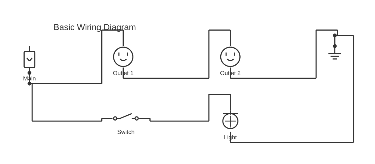
Schematic Diagram vs Block Diagram: Key Differences — circuit diagram showing component connectionsMainOutlet 1Outlet 2SwitchLightBasic Wiring Diagram
Schematic Diagram vs Block Diagram: Abstraction Levels, Design Hierarchy, and When to Use Each — interactive diagram. Open it in the editor to customise components and wiring.

This is a free printable schematic diagram vs block diagram: download the diagram as SVG or open it and print to paper or PDF.
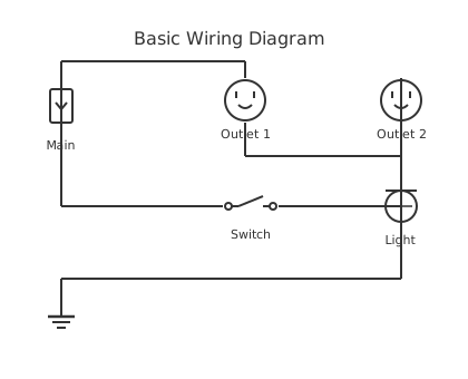
A schematic diagram shows individual electrical components — resistors, capacitors, transistors, relay coils — connected by lines representing electrical nodes, using standardised symbols defined by IEC 60617 or ANSI/IEEE 315. A block diagram represents the same system as labelled boxes (subsystems or functions) connected by lines or arrows showing signal flow or information transfer, without revealing component-level detail. The two diagram types are not alternatives to each other; they occupy different levels in the engineering design hierarchy, and professional electrical documentation normally contains both.

In the engineering design process, complexity is managed through abstraction. The design hierarchy runs from the most abstract level — the block diagram — down through the schematic diagram to the most concrete level, the wiring diagram. Each level answers a different question: the block diagram answers 'what does this system do and how do the parts relate?'; the schematic answers 'how does each circuit within that system work?'; the wiring diagram answers 'how do I physically wire it all together?' Understanding this hierarchy is the single most important conceptual gap in every competing page on this topic.

A block diagram uses simple geometric shapes — usually rectangles — to represent subsystems, functions, or major components. Each block is labelled with its function ('power supply,' 'amplifier stage,' 'microcontroller,' 'motor driver') rather than with component values. Lines or arrows between blocks represent connections, with the direction of the arrow indicating signal flow or information transfer. The internal workings of each block are deliberately hidden — this is the black-box principle: to understand how the audio amplifier system connects to its power supply and speaker load, you do not need to know whether the amplifier uses a class AB bipolar transistor output stage or a class D switching topology. The block diagram treats each subsystem as a black box: only its inputs and outputs are shown.

This abstraction serves multiple important purposes. In the concept and requirements phase of a project, before any component-level decisions are made, the block diagram allows the entire design team — engineers, project managers, purchasing, and non-technical stakeholders — to agree on the system architecture and the interfaces between subsystems. A hardware engineer can hand a block diagram to a software engineer and a mechanical engineer simultaneously; all three can read it and understand their interface responsibilities without knowing each other's technical discipline. This cross-discipline accessibility is precisely what the schematic — with its dense symbol vocabulary and implicit electrical knowledge — cannot provide.

Schematic diagrams are the working documents of electronics and electrical engineers. Every component has a standardised symbol defined by IEC 60617 (international) or ANSI/IEEE 315 (North American), a reference designator (R1, C3, U2), and an annotated value or part number. The schematic shows the full electrical behaviour: component values determine voltage division ratios, time constants, gain, impedance matching, and protection levels. A schematic for a power supply will show the transformer winding ratio, the rectifier diode part numbers, the filter capacitor values and voltage ratings, the voltage regulator IC and its feedback resistors — all the information needed to analyse whether the design meets its specification, to simulate it in LTspice, and to hand it to a PCB layout engineer.

The top-down design process moves from block diagram to schematic in a structured sequence. First, the system block diagram defines subsystem boundaries and interfaces. Next, each block is expanded into a schematic: the 'power supply' block becomes a full transformer-rectifier-regulator circuit; the 'amplifier' block becomes a transistor or op-amp circuit with gain-setting resistors; the 'microcontroller' block becomes a schematic sheet showing the MCU symbol, its decoupling capacitors, crystal oscillator, reset circuit, and peripheral connections. This progression from abstract to concrete is the fundamental method of managing complexity in electronic product design, and it is completely absent from every competing page on this topic.

Control system block diagrams deserve special attention because they are frequently encountered by engineers working on automation, process control, and power electronics, yet they are distinct from both system block diagrams and PLC function block diagrams. A control system block diagram represents a feedback control loop using standard control theory notation: a reference input, a summing junction (circle with + and − inputs), a forward-path transfer function G(s), a feedback-path transfer function H(s), and an output. The transfer function within each block is a mathematical expression (a Laplace transform, a gain, an integrator) rather than a circuit description. These diagrams are drawn to analyse stability, bandwidth, and transient response — they are the language of control engineers, not circuit engineers — but they frequently need to be translated into schematics (for analogue control circuits) or PLC programs (for digital control).

PLC Functional Block Diagrams (FBD), standardised by IEC 61131-3, are a third distinct type. In IEC 61131-3, FBD is one of five programming languages for PLCs. FBD programs are graphical: function blocks (AND gates, counters, timers, PID controllers) are connected by signal lines. They visually resemble electronic schematic diagrams but operate in the digital/software domain rather than the electrical domain. A PLC FBD program controls discrete inputs and outputs — sensors, actuators, motors — but the FBD diagram itself is not a schematic of any physical circuit; it is a program. The confusion between FBD (IEC 61131-3 PLC language), system block diagram (architecture document), and control system block diagram (control theory analysis tool) is a genuine source of confusion that no competitor resolves.

A worked example clarifies the hierarchy. Consider an audio power amplifier product. The system block diagram shows: AC mains input → power supply block → audio input block → preamplifier block → power amplifier block → speaker output. Signal flow arrows connect the blocks. No component values appear. This document is presented to the product manager, the regulatory engineer (for EMC pre-compliance discussion), and the PCB house quoting the job. The schematic for the power supply block then shows: mains inlet with fuse and varistor, toroidal transformer (turns ratio 230:22+22 V), full-bridge rectifier (four 1N5408 diodes), electrolytic reservoir capacitors (10,000 µF/50 V), and linear regulator ICs for the ±15 V rails. The schematic for the power amplifier block shows the output transistor pair (e.g., MJL3281A/MJL1302A), their bias circuits, the feedback network, and the output inductor and Zobel network. These two schematics together represent the complete component-level design. The wiring diagram then shows how to connect all the boards and the transformer inside the amplifier chassis.

From a stakeholder communication perspective: use a block diagram when presenting to non-engineers, at project kickoff, when defining interface specifications, or when documenting a product for a system-level technical manual. Use a schematic when performing circuit analysis, handing off to a PCB layout engineer, running SPICE simulation, writing a bill of materials, or producing compliance documentation. Knowing which is appropriate for the audience prevents under-communicating (handing a block diagram to a technician who needs to build the circuit) and over-communicating (presenting a 12-sheet schematic to a project manager who needs to understand the system architecture in five minutes).

Map out your system as a block diagram first, then drill down to a full schematic — all in the same free editor. No switching tools, no export headaches.

How to wire schematic diagram vs block diagram

  1. Start with the system block diagram Draw a high-level block diagram showing every major subsystem as a labelled rectangle. Define the signal flow arrows between blocks — what information or power passes between subsystems, in which direction, and at what interface level (voltage, current, data bus, protocol).
  2. Define interface specifications at block boundaries Before drawing any schematic, write down the interface specification for every connection between blocks: signal name, voltage range, current capacity, frequency, impedance. These constraints will drive the component-level design inside each block.
  3. Expand each block into a schematic Take one functional block at a time and design its internal circuit as a schematic. Choose component values to meet the interface specifications. Assign reference designators (R1, C1, U1) and add component values or part numbers. Keep the schematic for each block on its own sheet or page if the design is complex.
  4. Verify interfaces between schematics Check that the output of each block's schematic is compatible with the input of the next block's schematic. Verify voltage levels, impedances, and current drive capability at every interface point defined in step 2.
  5. Integrate and simulate For a system with analogue circuits, run SPICE simulation on the integrated schematic to verify gain, bandwidth, noise, and stability. For a digital or mixed-signal system, verify timing and signal integrity. Use the block diagram to structure the simulation — simulate one block at a time before integrating.
  6. Present block diagram to stakeholders Use the system block diagram (not the schematic) for reviews involving non-engineers, for management sign-off, and for interface agreement between teams. Bring schematics only to technical reviews with electrical engineers and PCB designers.
  7. Keep both documents updated through revisions Any architectural change that affects subsystem boundaries or interfaces must update the block diagram first. Any component-level change within a block updates the relevant schematic. Both documents must carry matching revision numbers and change descriptions in their title blocks.

Specifications

Abstraction levelBlock diagram: high — functions and subsystems as labelled boxes | Schematic: low — individual components with exact symbols, values, and reference designators
Detail shownBlock diagram: system topology, signal/data flow, subsystem interfaces | Schematic: component values, pin connections, voltage ratings, electrical behaviour
Symbols usedBlock diagram: simple rectangles and shapes with text labels | Schematic: standardised electrical symbols per IEC 60617 or ANSI/IEEE 315
Primary audienceBlock diagram: management, system architects, cross-discipline teams, stakeholders | Schematic: electronics engineers, PCB designers, controls technicians
Best forBlock diagram: concept design, system architecture, interface definition, overview documentation | Schematic: circuit design, PCB layout, SPICE simulation, troubleshooting, compliance documents
Shows electrical values?Block diagram: no — values are hidden inside each block | Schematic: yes — resistance, capacitance, voltage ratings, IC part numbers
PLC/automation variantBlock diagram: Functional Block Diagram per IEC 61131-3 (PLC programming language) | Schematic: ladder diagram or traditional schematic for relay/hardware control
Control system variantBlock diagram: control system block diagram with transfer functions G(s), H(s), feedback loops | Schematic: analogue circuit schematic implementing the controller
StandardsBlock diagram: no universal electrical symbol standard; IEC 61131-3 for PLC FBD | Schematic: IEC 60617, ANSI/IEEE 315
Created when in design processBlock diagram: early phase — concept and requirements | Schematic: detailed design phase, after block diagram is approved
Interchangeable?No — they operate at different abstraction levels and serve different audiences and purposes

Safety warnings

Tools needed

Common mistakes

Troubleshooting

Block diagram and schematic describe different system architectures
Cause: The schematic was modified during detailed design (e.g., a subsystem was split in two, or two functions were merged into one IC) without updating the block diagram. Fix: Reconcile by using the schematic as the definitive technical reference. Redraw the block diagram to accurately reflect the subsystems as implemented in the schematic. Note the discrepancy in the revision history of both documents.
Signal level at block boundary not met in the schematic implementation
Cause: The interface specification defined at the block diagram level (e.g., '5V CMOS output, 10 mA drive') was not carried through to the schematic component selection, or a component was substituted with one that has different drive capability. Fix: Trace the interface signal from the source block's output circuit to the destination block's input circuit on the schematic. Verify output drive capability and input threshold from component datasheets. Add a buffer or level-shifter stage if required, and update the schematic and block diagram interface specification accordingly.
PLC FBD program behaves differently from the control system block diagram specification
Cause: The transfer function or logic described in the control system block diagram was implemented incorrectly in the FBD (wrong gain, missing integrator reset, incorrect discrete-time approximation of a continuous-time controller). Fix: Compare the FBD program block-by-block against the control system block diagram. Verify that every transfer function, gain, and time constant is correctly represented in the PLC function blocks. Re-tune using the PLC's offline simulation mode before deployment.
Block diagram presented to management shows incorrect interfaces after design change
Cause: A design change was made at the schematic level and the block diagram was not updated, leaving the architectural document out of sync with the actual implementation. Fix: Establish a design change procedure that requires block diagram review as a mandatory step whenever a schematic change affects subsystem boundaries or inter-block interfaces. Update both documents simultaneously and issue under the same revision letter.

Frequently asked questions

What is the main difference between a block diagram and a schematic?

A block diagram shows a system's subsystems and their relationships as labelled boxes, hiding internal component detail. A schematic shows the individual electrical components — and their values, symbols, and connections — that make up the circuit inside each block. Block diagrams operate at the system level; schematics operate at the component level.

Which comes first in the design process — block diagram or schematic?

The block diagram comes first. In top-down design, the system is decomposed into functional blocks before any component-level decisions are made. Once the block diagram is agreed upon and the interfaces between blocks are defined, engineers create schematics for each individual block. This sequence prevents designing components that don't communicate with each other correctly.

Can a block diagram replace a schematic in documentation?

No. A block diagram alone cannot be used for circuit analysis, PCB layout, SPICE simulation, bill of materials creation, or compliance documentation (CE, UL). It is an architectural overview, not a design specification. Professional documentation packages contain both: a system block diagram for architecture and individual schematics for implementation.

What is a functional block diagram (FBD) in PLC programming?

Functional Block Diagram (FBD) is one of the five IEC 61131-3 programming languages for Programmable Logic Controllers. It represents the PLC program graphically as interconnected function blocks (AND gates, timers, counters, PID controllers). Despite its visual resemblance to an electrical schematic or system block diagram, an FBD is a software program, not a circuit drawing, and it runs inside a PLC to control physical outputs.

What is a control system block diagram?

A control system block diagram represents a feedback control loop using transfer functions (mathematical expressions in the Laplace domain), summing junctions, and signal flow arrows. It is used by control engineers to analyse stability, bandwidth, and transient response. It is distinct from a system architecture block diagram (which uses descriptive text labels) and from a PLC FBD program (which is executable software).

What software is used to draw block diagrams vs schematics?

Block diagrams are commonly drawn in draw.io (free), Microsoft Visio, Lucidchart, or the block diagram tools in circuitdiagrammaker.com. Schematics require an electrical symbol library: KiCad (free, open-source), Altium Designer, Eagle CAD, or circuitdiagrammaker.com for browser-based schematic drawing with IEC and ANSI symbols.

Is a block diagram an electrical diagram?

Not necessarily. Block diagrams are used in many disciplines — software architecture (UML), process engineering (P&ID at a high level), control theory, and systems engineering — not just electrical engineering. A block diagram used to represent an electrical system is an electrical document, but the format itself is discipline-neutral. A schematic, by contrast, is always an electrical diagram.

How do I convert a block diagram into a schematic?

Take each functional block and expand it into a full schematic subcircuit. Define the interface signals at the block boundaries (voltage levels, signal types, impedances) and use those as constraints when designing each subcircuit. Assign reference designators to every component in each block's schematic. The completed set of subcircuit schematics, taken together, is the schematic implementation of the block diagram.

Related diagrams

Free electrical calculators

Edit this diagram free in the online editor