Schematic to Breadboard and PCB Workflow
Quick answer: A schematic can become a useful breadboard or PCB starting point only when every placed symbol has a compatible physical package and a verified pin mapping. The conversion should preserve nets, surface unmapped parts, check placement connectivity, and make the limits of the physical model explicit.
User job: Move a supported electronic schematic into prototype and two-layer physical views without retyping connectivity.
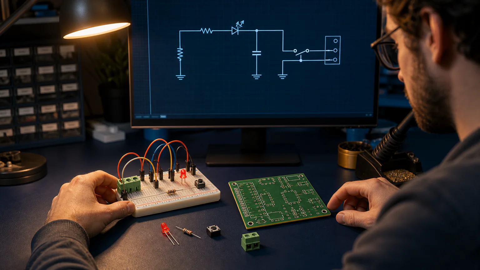


Worked example
A low-voltage LED driver built from a source, resistor, LED, switch and connector can map to through-hole packages, generate a breadboard placement, and create a PCB Lite starting point while keeping the same component references and nets.
Step-by-step workflow
- Finish and electrically check the schematic
- Attach compatible physical packages and verify pin maps
- Generate the breadboard placement and inspect every jumper
- Open PCB Lite, place footprints and review two-layer routing
- Export the supported manufacturing-review package and verify it externally
Outputs and deliverables
- Pin-aware schematic
- Connectivity-aware breadboard layout
- Through-hole footprint set
- Two-layer PCB Lite starting point
- BOM, positions, drill and supported Gerber outputs
Quality checks before issue
- Every schematic pin maps to the intended physical pin
- Unsupported or unmapped parts block blind conversion
- Breadboard rows and rails preserve the netlist
- PCB outline, drills and clearances are reviewed
- Fabrication outputs match the released source project
Current product and engineering boundaries
- Not every schematic symbol has a physical package.
- Breadboard placement does not model every parasitic, current, thermal or high-frequency effect.
- PCB Lite does not provide copper zones, controlled impedance, panelization, native STEP/Parasolid exchange or manufacturer DFM certification.
Reviewed 2026-07-30: Product capabilities are first-party facts. Engineering examples are educational and must be verified for the actual project, equipment and jurisdiction.
Frequently asked questions
What is Schematic to Breadboard and PCB Workflow used for?
A schematic can become a useful breadboard or PCB starting point only when every placed symbol has a compatible physical package and a verified pin mapping. The conversion should preserve nets, surface unmapped parts, check placement connectivity, and make the limits of the physical model explicit.
What does this workflow produce?
Pin-aware schematic, Connectivity-aware breadboard layout, Through-hole footprint set, Two-layer PCB Lite starting point, BOM, positions, drill and supported Gerber outputs.
What should be checked before using the result?
Every schematic pin maps to the intended physical pin Unsupported or unmapped parts block blind conversion Breadboard rows and rails preserve the netlist PCB outline, drills and clearances are reviewed Fabrication outputs match the released source project
What does CircuitDiagramMaker not automate here?
Not every schematic symbol has a physical package. Breadboard placement does not model every parasitic, current, thermal or high-frequency effect. PCB Lite does not provide copper zones, controlled impedance, panelization, native STEP/Parasolid exchange or manufacturer DFM certification.
Can I continue with an editable project?
Yes. The page links to the closest supported editor, template, calculator, component library, or engineering workspace action.
Open a compatible prototype project or inspect the current product capability matrix.